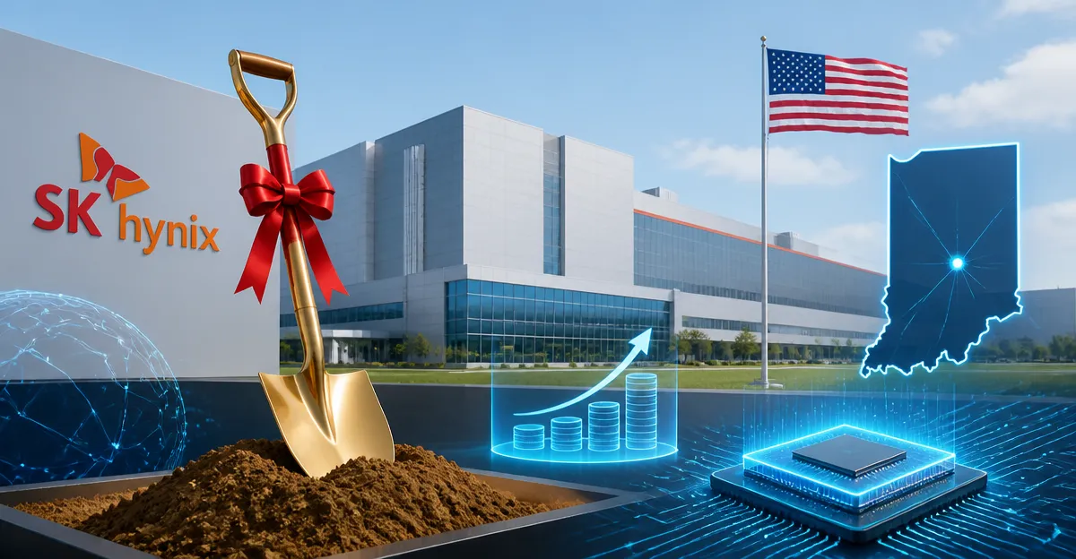
August 27, 2026, (Inside AI) — SK Hynix broke ground Thursday on a $4 billion advanced chip packaging and research facility in West Lafayette, Indiana, a move that deepens U.S. AI memory production and shortens supply lines to key customers like Nvidia, Microsoft, and Google.
The ceremony at Purdue Research Park marks a formal start to construction, with cleanroom operations slated for the second half of 2028. The site will host a next-generation high-bandwidth memory (HBM) packaging line and an AI semiconductor R&D hub, according to company statements.
The investment is part of a broader push to localize AI memory production near major U.S. buyers and to tap Purdue’s engineering talent. SK Hynix expects the project and related supply-chain investment to create about 7,000 direct and indirect local jobs.
“The project will add advanced packaging capacity in the United States at a time when AI investment is driving rapid growth in demand for HBM,” the company said in a statement.
HBM’s Pricing Power Reshapes Memory Economics
HBM stacks memory chips vertically to deliver faster data processing with lower power use, making it essential for AI accelerators. Unlike conventional DRAM, HBM is tightly integrated with AI processors, raising technological barriers and giving suppliers stronger pricing leverage.
SK Hynix controlled 58% of global HBM revenue in the first quarter of 2026, according to Counterpoint Research. Samsung Electronics and Micron Technology each held 21%.
That dominance is reflected in the scale of the Indiana project. SK Hynix initially announced a $3.87 billion investment in 2024, but the total has since climbed above $4 billion. The U.S. government finalized $458 million in grants and up to $500 million in loans under the CHIPS Act in December 2024.
Separately, SK Hynix’s board approved about 54.3 trillion won ($38.30 billion) of investments through 2031, including 35.2 trillion won for a second phase of fab construction in South Korea.
Nvidia’s Forecast Adds Urgency to U.S. Packaging
Nvidia on Wednesday projected a 70% revenue jump in the next fiscal year, signaling that AI demand remains robust even as memory shortages constrain expansion. That backdrop makes SK Hynix’s U.S. packaging capacity strategically significant.
The Indiana facility will not produce HBM wafers; it will package them, a critical step where chips are stacked and connected to AI processors. By moving that step closer to U.S. customers, SK Hynix aims to reduce logistics risk and support just-in-time supply for data center builders.
Industry analysts note that advanced packaging has become a bottleneck. TSMC and Intel are also expanding U.S. packaging capacity, but HBM-specific lines remain scarce. SK Hynix’s move could pressure rivals to follow.
The company’s research ties with Purdue are expected to focus on advanced packaging materials, thermal management, and heterogeneous integration. Purdue already hosts a major semiconductor innovation hub, and the partnership may yield a pipeline of engineers for the new facility.
For Indiana, the project reinforces a growing semiconductor corridor. The state has attracted multiple chip investments in recent years, including a $1.8 billion SkyWater Technology fab and a $3.5 billion NHanced Semiconductors advanced packaging plant.
SK Hynix did not disclose specific production capacity targets for the Indiana site. However, the company’s broader investment plan suggests a multi-year effort to defend its HBM lead and meet AI-driven memory demand through the end of the decade.