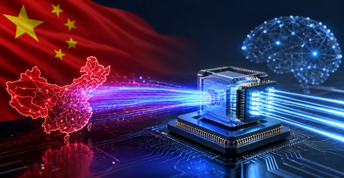
July 13, 2026, (Inside AI) — A team of Chinese researchers has unveiled an all-optical interconnect system that accelerates AI distributed inference by over 100 times while slashing computational resource usage to just one-ninth of conventional methods. The breakthrough, published in the journal National Science Review, links standard electronic chips via custom silicon photonic components, sidestepping the need for exotic hardware.
The system’s core innovation lies in its optical “joints” that replace traditional electrical interconnects. A 400 Gbps silicon photonic transceiver chip handles the conversion between electrical and optical signals, while a dedicated optical network-on-chip orchestrates data flow. This architecture eliminates the bandwidth bottlenecks that plague copper-based interconnects, enabling near-instantaneous communication between field-programmable gate arrays (FPGAs).
Corresponding authors Shu Haowen and Wang Xingjun from Peking University led the effort. Their work addresses a pressing industry pain point: as AI models balloon in size, the energy and latency costs of shuttling data between processors have become untenable. Traditional scaling relies on adding more GPUs and building larger data centers, but this brute-force approach is hitting physical and economic limits.
“This optical interconnect system fundamentally changes the cost structure of distributed inference,” said an independent researcher not involved in the study. “By decoupling communication from electronic constraints, they’ve achieved a step-function improvement in efficiency.”
Read: Why AI’s Next Chapter Belongs to CPUs: The Shift to Efficient Inference
The researchers validated their design using a cluster of FPGAs running a transformer-based model. The optical links maintained 99.5% of the accuracy of a single-chip system while processing data 100 times faster than an equivalent electrical setup. Crucially, the system required only 11% of the computational resources typically needed for the same workload.
This isn’t the first foray into optical computing. Silicon photonics has long promised faster, cooler data movement, but integrating it with commodity electronics has proven stubbornly difficult. Previous efforts often required custom processors or operated at impractically small scales. The Peking University team’s breakthrough lies in its compatibility with off-the-shelf FPGAs, making it a drop-in upgrade for existing infrastructure.
However, significant hurdles remain before this technology reaches cloud data centers. The current prototype uses discrete components that must be miniaturized and packaged for mass production. Reliability testing over thousands of hours is still needed, and the cost of silicon photonic fabrication remains higher than traditional PCB traces.
Industry reactions have been cautiously optimistic. “This is a promising proof of concept, but the path from lab to deployment is long,” said Dr. Li Wei, a photonics researcher at Tsinghua University. “The real test will be whether they can maintain this performance at scale with thousands of nodes.”
The timing is critical. Global demand for AI inference is projected to grow 30% annually, pressuring energy grids and supply chains. Optical interconnects could reduce the carbon footprint of large-scale AI by an order of magnitude, aligning with stricter environmental regulations in the European Union and China.
The paper’s digital object identifier is 10.1093/nsr/nwae215, providing full technical details. The team is now working on integrating the optical transceivers directly onto FPGA packages, aiming for a commercial prototype within two years.
Read: Chinese Team’s Brain-Mimicking Chip Is Up to 478 Times Faster Than Nvidia GPU
While the 100-fold speedup grabs headlines, the resource efficiency is arguably more transformative. It suggests that future AI clusters could be built with fewer, cheaper chips, democratizing access to powerful inference. For an industry caught between insatiable demand and physical limits, this optical detour may be the only viable path forward.