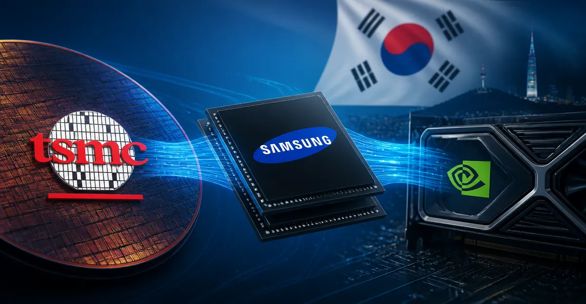
October 18, 2026, (Inside AI) — Samsung Electronics will use Taiwan Semiconductor Manufacturing Company's 3-nanometre process to produce base dies for Nvidia's next-generation custom high-bandwidth memory chips, according to a report in the Seoul Economic Daily. The move would mark the first time Samsung has worked with the Taiwanese contract chipmaker at the HBM manufacturing stage, the newspaper said. The report did not specify which Nvidia product line would use the chips or when production would begin.
The arrangement would represent a significant shift in the semiconductor supply chain. Samsung, the world's largest memory maker, has historically produced its own base dies for HBM. Using TSMC's 3nm technology for the logic layer of Nvidia's custom HBM would make Samsung dependent on a direct competitor for a critical component. The base die controls data flow between the memory stacks and the GPU, and its manufacturing process affects power efficiency and performance.
Samsung's Unusual Concession to a Foundry Rival
Nvidia's HBM requirements have grown more demanding with each GPU generation. The company's custom HBM designs require base dies tailored to its specifications, and TSMC has become the preferred foundry for those logic layers. SK Hynix, Samsung's main HBM rival, already uses TSMC for base dies in some products. Samsung's decision to follow that path suggests the company prioritizes winning Nvidia's business over protecting its internal foundry operations.
The report did not name the specific Nvidia product that would use the Samsung-TSMC HBM. Nvidia's next-generation GPUs, likely the Rubin architecture, are expected to require HBM4 memory. HBM4 specifications call for wider interfaces and higher bandwidth than current HBM3E, making the base die more complex and more valuable. TSMC's 3nm process offers density and power advantages over Samsung's own foundry nodes, according to industry analysts.
Inside AI could not independently verify the report. Samsung and TSMC declined to comment on the matter. Nvidia did not respond to a request for comment.
This development carries strategic weight beyond a single component. Samsung's foundry business has struggled to attract major customers, while TSMC dominates advanced logic manufacturing. By allowing TSMC to produce base dies for Nvidia's HBM, Samsung effectively acknowledges that its own foundry cannot meet Nvidia's requirements for this specific application. The move could deepen Samsung's reliance on TSMC and complicate its long-term ambition to challenge TSMC in advanced packaging and logic.
For Nvidia, the arrangement diversifies its HBM supply chain. The company currently sources HBM primarily from SK Hynix and Micron. Adding Samsung with TSMC-made base dies could increase supply and reduce risk. Nvidia's GPU production has been constrained by HBM availability in recent years, and the company has pushed suppliers to expand capacity.
Read: Nvidia, Broadcom Shielded as AI Power Crunch Hits Chip Supply Chain, Says Morgan Stanley
The Seoul Economic Daily report follows a pattern of Samsung seeking external foundry help for advanced packaging. In 2025, Samsung used TSMC for some interposer production, according to industry sources. The latest move extends that collaboration to the HBM base die, a more central component.
Market reaction was muted. Samsung shares closed slightly lower in Seoul trading on Friday, before the report was published. TSMC shares were unchanged. Analysts said the news confirms Samsung's pragmatic approach but raises questions about its foundry roadmap.
Samsung has not announced a timeline for the Nvidia HBM production. The company is expected to begin mass production of HBM4 in 2027, according to its public roadmap. Whether the TSMC-made base dies will be used in that initial production remains unclear.