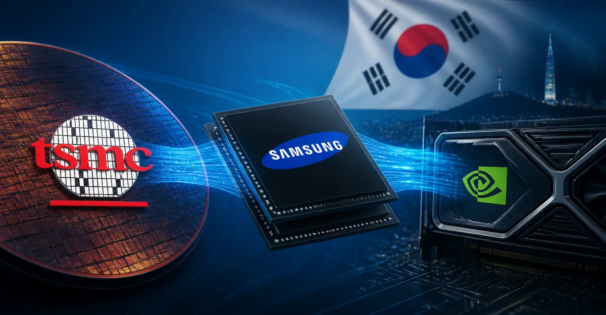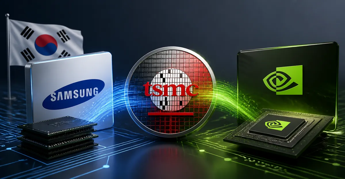
October 19, 2026, (Inside AI) — Samsung Electronics will produce base dies for Nvidia's next-generation high-bandwidth memory (HBM) chips using TSMC's 3-nanometre process, according to a report by the Seoul Economic Daily. The arrangement would mark the first time Samsung has collaborated with the Taiwanese contract chipmaker at the HBM manufacturing stage. Nvidia has reportedly asked all three major memory suppliers, Samsung, SK Hynix, and Micron Technology, to adopt TSMC's process for NVHBM base dies and sixth-generation DRAM technology for core dies.
The shift underscores Nvidia's push to standardize its memory supply chain for next-generation AI accelerators. NVHBM, unveiled in August, integrates Nvidia's custom memory controller directly into the base die. This design aims to ensure consistent implementation across multiple memory vendors, reducing integration complexity for Nvidia's customers. Samsung's acceptance of these requirements, after an internal review, signals a significant strategic adjustment. The company will retain its in-house production model for standard HBM and custom products for other clients, but it is also assessing whether its own foundry could produce NVHBM base dies if demand exceeds TSMC's capacity, according to an unnamed source cited in the report.
Samsung's Foundry Dilemma Deepens
The decision highlights the growing interdependence in the semiconductor industry, where even fierce rivals must collaborate to meet the demands of AI computing. Samsung's foundry business has lagged behind TSMC in advanced node yields, making the Taiwanese firm the preferred choice for critical components. By outsourcing base die production to TSMC, Samsung ensures its memory products remain compatible with Nvidia's specifications, but it also cedes a portion of the value chain to a competitor. This dynamic could accelerate the consolidation of advanced chipmaking around TSMC, further entrenching its dominant position.
Nvidia's move to standardize NVHBM across suppliers is a departure from its previous approach, where memory vendors had more flexibility in designing base dies. The integration of Nvidia's memory controller into the base die allows for tighter optimization between the GPU and memory, potentially delivering performance gains for AI workloads. The requirement for sixth-generation DRAM technology in core dies also pushes suppliers to accelerate their roadmaps. Samsung, SK Hynix, and Micron are all racing to develop and qualify next-generation DRAM, with SK Hynix currently leading in HBM market share.
Read: Samsung Q3 profit jumps nearly nine-fold as AI memory boom lifts chip earnings
The report did not specify a timeline for production or the financial terms of the arrangement. Samsung and TSMC have not publicly commented on the matter. Nvidia declined to comment on the report. The collaboration, if confirmed, would represent a notable shift for Samsung's foundry strategy, which has historically emphasized in-house production for its memory products. It also raises questions about capacity allocation at TSMC, which is already juggling demand from Apple, AMD, and other major customers.
Industry analysts suggest that Nvidia's decision to mandate TSMC's process for NVHBM base dies could set a precedent for future memory generations. By standardizing the base die, Nvidia simplifies its validation and qualification processes, reducing time-to-market for new AI systems. However, it also reduces the differentiation that memory vendors can offer, potentially leading to a more commoditized HBM market. Samsung's willingness to comply, despite the competitive implications, reflects the importance of securing Nvidia as a customer. Nvidia dominates the AI accelerator market, and its memory requirements are massive.
The move also underscores the challenges facing Samsung's foundry business. Despite heavy investment, Samsung has struggled to win major customers for its advanced nodes, with many opting for TSMC's more mature ecosystem. The NVHBM deal, while a win for TSMC, could provide Samsung with valuable experience in advanced packaging and integration, which it could apply to its own foundry offerings in the future. The unnamed source's mention of Samsung assessing its own foundry for NVHBM base dies suggests the company is keeping its options open.
Read: Nvidia, Broadcom Shielded as AI Power Crunch Hits Chip Supply Chain, Says Morgan Stanley
For now, the industry watches as Nvidia tightens its grip on the AI hardware stack, from GPUs to memory interfaces. The NVHBM standard, if widely adopted, could become a key building block for next-generation AI systems, and the suppliers who adapt fastest will reap the rewards. Samsung's decision to use TSMC's 3nm process is a pragmatic step, but it also highlights the strategic tightrope the company walks between its memory and foundry ambitions.